ABOUT THE PROJECT
In places where electricity is not available, a portable
electric generator and a battery are alternative power sources.
The latter is cheaper than the electric generator, can easily be
recharged, and does not require elaborate maintenance procedure.
Unfortunately, a car battery is a DC source limited to a
potential of 12 volts. To convert this to a 220-volts
alternating current, a DC to AC inverter is necessary.
A power
inverter such as this featured project can be used. Its circuit
is simple. Requiring only two integrated circuits, four small
power transistors, and two power transistors as active elements.
Only the transformer is bulky and costly. The inverter can
safely supply power to 120-watt load.
Back to Top
The complete schematic diagram of the power inverter is shown in figure 1A. By function, it can be classified as mainly consisting of an astable oscillator, a flipflop circuit that generates pulse with opposite logic states at its Q and Q outputs, a switching circuit and a step-up transformer as shown in Figure 1B.

Fig 1B. Functional Diagram of the Power Inverter project.
The astable oscillator is configured around a 555 timer IC. Its
oscillating frequency is set to 120Hz by R1, R2, R3 and C1. the
resulting output is a train square waves having a peak to peak amplitude
nearly equal to the12 – Volts supply voltage. The way this oscillator
works can be easily understood through Fig. 2.
Figure 2. Internal block diagram of
the 555 timer IC.

Immediately upon application of the 12-volt supply voltage, the
voltage across capacitor C1 is nearly at the ground level. This voltage
sensed by the “trigger” comparator (pin2) of the timer, setting the
internal flip flop and hence, causing the output voltage at (pin3) to go
high or approximate the supply voltage. Consequently , it turns off the
“discharge” transistor and allowing capacitor C1 to charge through
resistors R1, R2 and R3. The capacitor charges towards the supply
voltage but upon reaching 2/3 of the supply voltage, the threshold
comparator (pin6) is activated. This causes the ineternal flip flop to
reset and the output voltage to go back to ground level. The discharge
transistor then conducts, which in turn, causes capacitor C1 to
discharge through R2 and R3 until the voltage across it drops to 1/3 of
the supply voltage, a level at which the “trigger” comparator switches
the timer output to a high state (or near the supply voltage level)
again, then the cycle is repeated.
The output of the oscillator is fed to the clock input of the 74C74
D-type flip flop. This IC has a dual function. First it divides equally
into two the timer frequency to obtain the nominal 60Hz output, and
secondly, it simultaneously provides complementary outputs (at its pins5
& 6) required by the succeeding switching circuit.
The part of the switching circuit that receives the flip flop outputs
are composed of buffer transistors Q1 and Q2. Resistors R4 and R5 limit
the current of the base of these transistors to a safe value. Resistors
R6 and R7 serve as pull up resistors that set the collector bias of
these transistors.
The output of the buffer transistors are in turn
connected to the push pull transistors consisting of the Q3-Q4 and Q5-Q6
pairs. The PNP transistors Q3 and Q5 act as driver transistors to Q4 and
Q6, respectively. They supply the current requirements of the main power
transistors so that the full saturation can be attained. The currents
supplied by these drivers can go up to five amperes depending on the
load connected the output of the inverter.
Transistors Q4 and Q6, wired in a push pull mode,
alternately supply current through each half of the primary winding of
the transformer. Alternate conduction here means when one transistor is
fully saturated, the other one is at cut off, and vice versa. This
alternate switching of the two transistors creates a magnetic field on
the transformer core resulting to a transfer of energy from the
secondary winding of the primary winding, a process termed as magnetic
induction. The power available at the secondary of the transformer has
been translated already to 220 volts alternating current in the form of
square waves. The primary to secondary winding turns ratio causes the
12-volt primary voltage to be stepped up to 220 Volts in the secondary
winding.
Back to Top

Fig 1A. Schematic diagram of the Power Inverter. Use AWG#10 wire for
the heavy line connections.
Back to Top
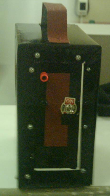
The
power inverter although composed of only a few components handles
large amounts of current thus necessitating extra precautionary
measures:
Use only AWG#10 insulated wire in
wiring connections indicated by heavy lines in Figure 1A. Use similar
wire size for connections to the battery.
Transistors Q4 and Q6 must be mounted
on a heatsink sufficient enough to dissipate the expected heat that may
be generate. A fin type heatsink is specifically recommended for this
purpose.
Transistors Q4 and Q6 must be both electrically isolated from the
heatsink
The rest of procedures are mainly a matter of following good
construction techniques as in doing other electronic projects:
1. Secure
the ready made PCB (See Figure 3 and 4). Carefully check the foil
path.
2. Insert and solder the components intended for the PCB. Take
note of the lead polarity or lead orientations of the electrolytic
capacitors and the transistors.
Capacitors C4 is mounted at the foil
side of the PCB at the location indicated in figure 4. Resistors R10
to R13 are not mounted in the PCB, refer to Figure 6.
3.
Mount the power transistors on the heatsink. If the heatsink is
to be grounded be sure to put mica insulators between the
heatsink and the power transistors.
4. Plan
the over all work to be done to complete the project with emphasis on
the layout in the enclosure of the PCB, transistors on the heatsink, and
the transformer.
Note:
do the wiring connections as illustrated in the wiring guide after the
TESTING procedures.


Figure 3. Foil pattern layout of
Figure 4. parts placement guide of
the Power Inverter.
the Power
Inverter.
*C4
is soldered at the foil side of the PCB at the location indicated.
Back to Top
Power Inverter
Parts List
Semiconductor :
IC1
- 555, Timer IC
IC2
- 74C74, CMOS DUAL D Flip Flop
Q1,Q2
- 9418, NPN Transistors
Q3,Q5 - NA52W, PNP 40W 45V 4A Transistors
Q4,Q6
- MJ15015, NPN 180W 120V 15A Transistors
Resistors : (All are 1/4 watt +-5% tolerance Carbon composition type, unless otherwise noted:)
R1 - 10 Kilohms
R2,R3 - 27 Kilohms
R4,R5 - 3.3 Kilohms
R6,R7 - 1 Kilohm
R8,R9 - 47 Ohms, 1 watt
R10,R11
- 330 Ohms
R12,R13 - 15 Ohms, 1/2 watt
Capacitors:
C1,C2
- 0.1uF/50V mylar
C3
- 220uF/25V electrolytic
C4
- 4.7uF/16V electrolytic
Miscellaneous:
SI-SPST 15 Amp Switch
Transformer - 24V CT Primary/220VSecondary, 150-watt
IC Socket, ICU - 8 - 1pc.
IC Socket, ICU - 14 - 1pc
Heatsink(fin type) - 9inches in length
Mica insulators - 2 pcs
Binding Posts - 1 pair
Car Battery Alligator Clips(red & black) - 1 pair.
Banana Plugs (red & black) - 1 pair.
AC Outlet, (chassis-mounted) - 1 pair.
PCB, Eyelets, Nuts and Bolts
AWG#10 and AWG#22 Insulated Hook-Up Wires, etc.
Back to Top
The
main function of the power inverter is to make available AC power in
instances when and where electricity is not available. This inverter
can supply power to any non critical appliance provided that its
power rating is within the 120-Watt level. However, since the output
of this inverter is a square wave and not sinusoidal as the supplied
house current, the inverter could not be used for TV and similar
electronic appliances. (Note: We have actually tested this inverter
using a TV load and encountered no problem at all. But this is not a
guarantee, however, that the same results will be obtained with
other TV brands. Some may performed as well or better but others may
be damaged when powered by a square wave AC source.)
Some
possible applications of the power inverter are the following:
1.
Lamps (fluorescent or incandescent)
2. Electric fan
3.
Low wattage heating applianced (120 watts maximum)
Back to Top
Item
Quantity
Price(P)
AWG#22
4m
10
P. Inverter Kit
1 kit
1282.50
Battery Clip
1pair
25
Footings
4 pcs.
8
Screws 1/8 x 1/2 20 pcs.
15
Heatsink 12"
12"
155
TW#10
2 m 73
Housing
450
Paint
25
Transportation
2 times
250
TOTAL COST
2293.50
Back to Top

Low
on minutes? You
may be able to "buy
some time" by watching
ads
Read more
|

This voice remote
hears your every
command. Now we're
talking.
Read more
|

One study claims
that frequent cell
users can suffer
from hearing loss.
Read more
|
Back to Top
Posted by Randy
 In places where electricity is not available, a portable electric generator and a battery are alternative power sources.
 NCST
NCST

.jpg)